Lorem ipsum dolor sit amet, consectetuer adipiscing elit. Aenean commodo ligula eget dolor. Aenean massa. Cum sociis natoque penatibus et magnis dis parturient montes, nascetur ridiculus mus.
Lorem ipsum dolor sit amet, consectetuer adipiscing elit. Aenean commodo ligula eget dolor. Aenean massa.
Lorem ipsum dolor sit amet, consectetuer adipiscing elit. Aenean commodo ligula eget dolor. Aenean massa.
Lorem ipsum dolor sit amet, consectetuer adipiscing elit. Aenean commodo ligula eget dolor. Aenean massa.
Lorem ipsum dolor sit amet, consectetuer adipiscing elit. Aenean commodo ligula eget dolor. Aenean massa. Cum sociis natoque penatibus et magnis dis parturient montes, nascetur ridiculus mus. Donec quam felis, ultricies nec, pellentesque eu, pretium quis, sem.
Euismod, quis laoreet neque imperdiet. Proin ornare, orci eu mattis dignissim, mi mauris consectetur dui, at faucibus libero justo a dui. Sed facilisis pellentesque quam et blandit.


Tessolve is a special Engineering Services company that able to bring you a different path to solve your problems . Solutions from Lumissil/Ingenic ; MediaTek , Alif Semi and more that drives Embedded Innovation .


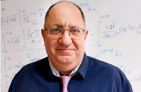
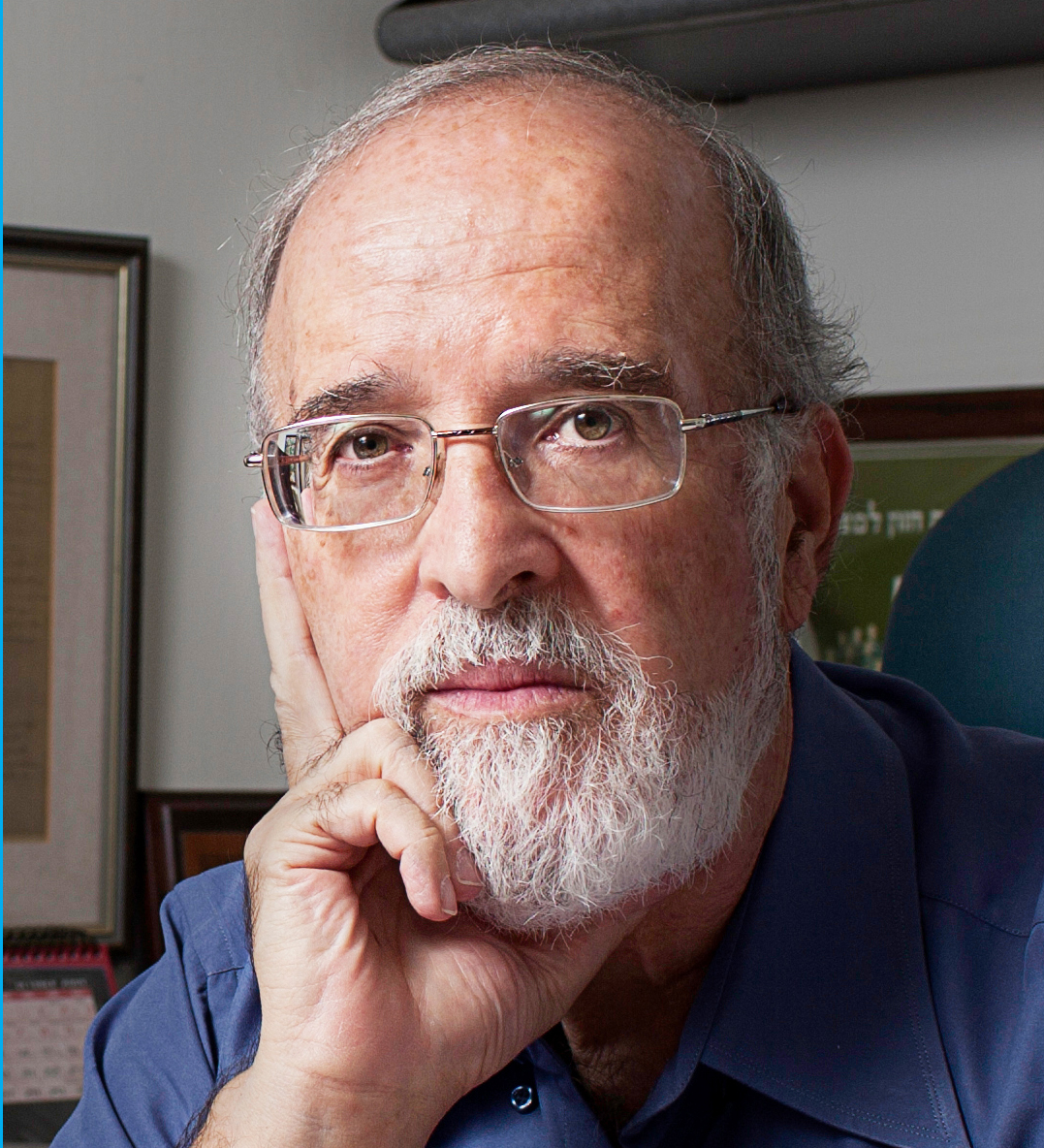
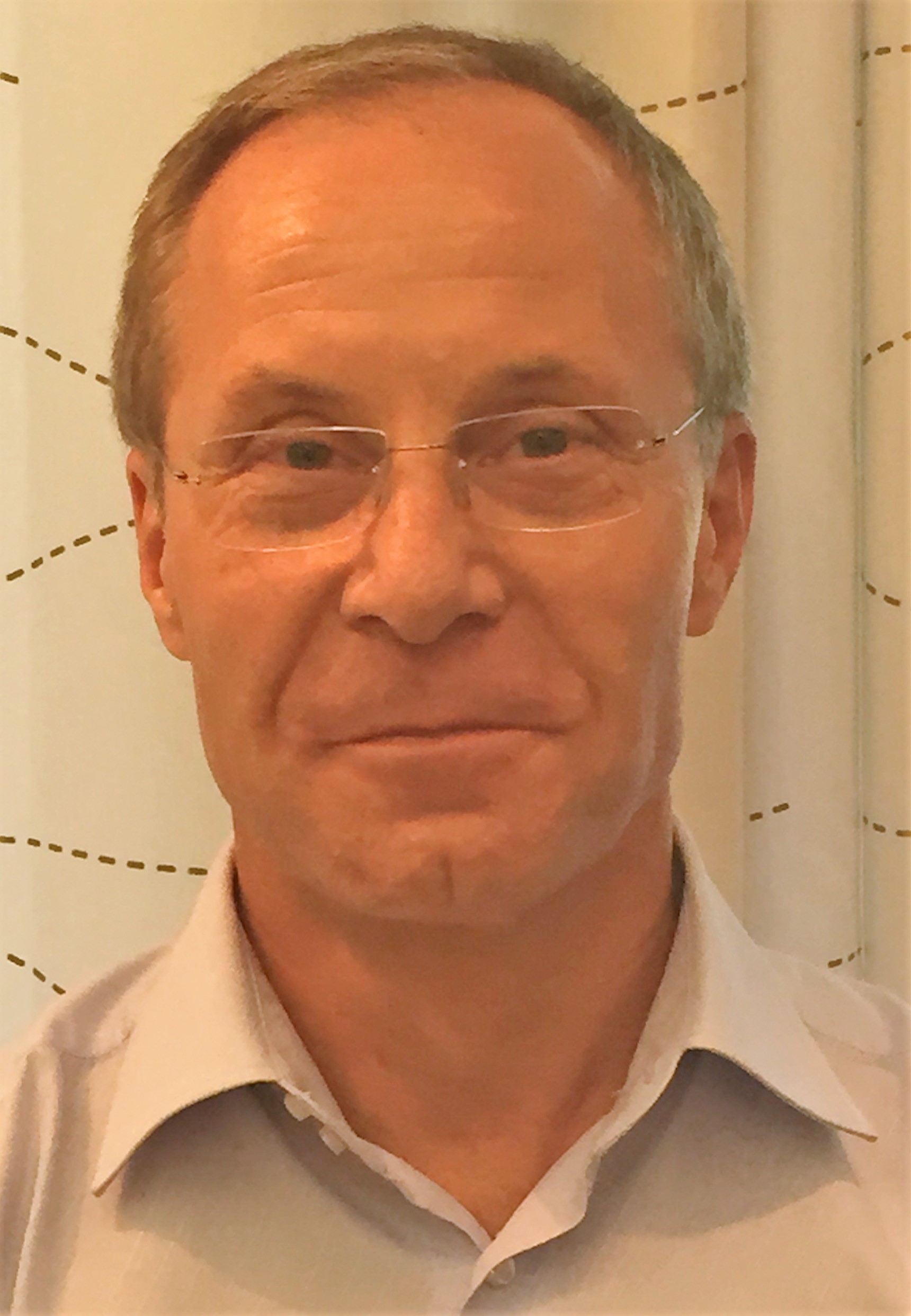
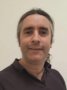
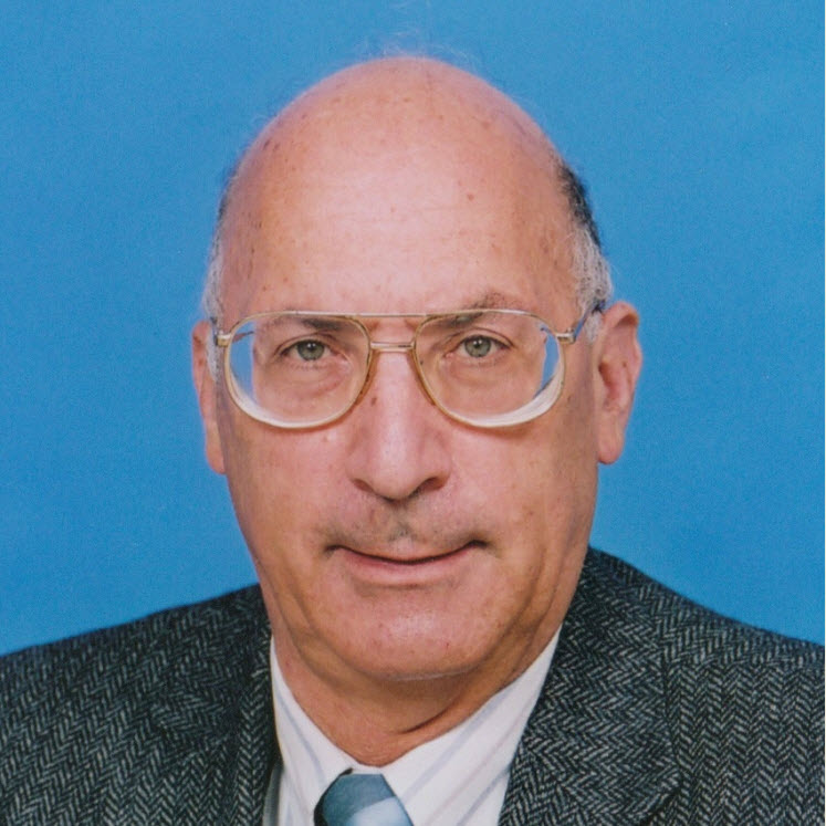
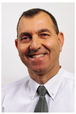
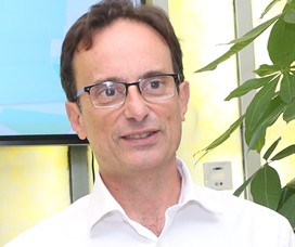
Prof. Dan Sadot, Chairman of the Cathedra for Electro-optics at Ben Gurion University
Current trends in underwater wireless optical communication

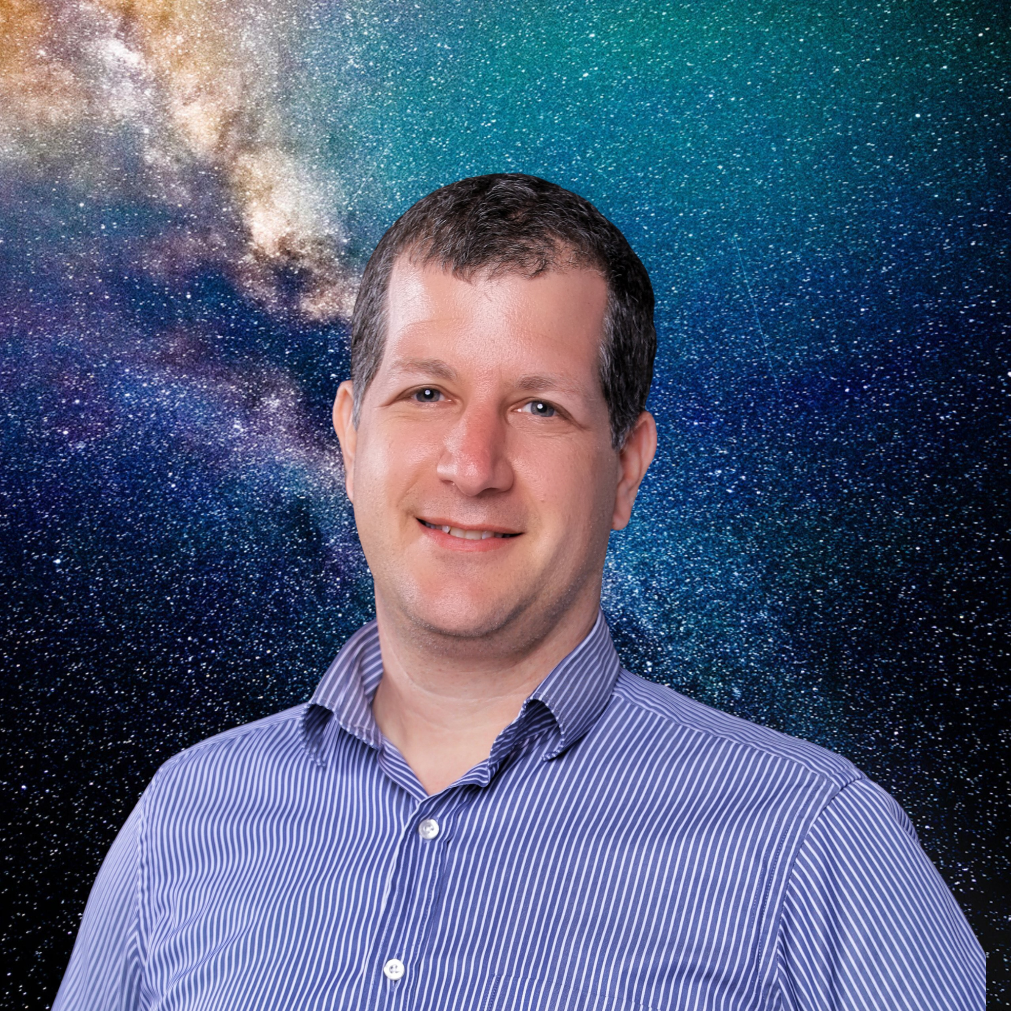
High Energy Astrophysics


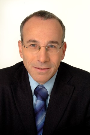
The present status of Wide Band Gap (WBG) Transistors: characterization and uses Recent introduction of WBG transistors is revolutionizing Power Electronics by making possible the design of more efficient and smaller power converters and inverters, thanks to the lower switching and conduction losses of SiC and GaN devices. In this lecture, the characterizations and practical applications of these devices will be discussed along with guidelines for drive, protection and parallel operation.
Power electronics challenges and solutions of e-Mobility: E-Mobility design is under pressure for a major makeover due to tighter regulations, very large increase in demand, the pressure to improve efficiency and control, reduce cost, and minimize battery charging time. The solution to many of these challenges are within the power electronics domain which is now helped by the introduction of new power electronics devices such as Wide Band Gap (WBG) transistors. These issues will be discussed with examples in this lecture.


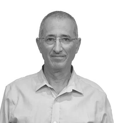
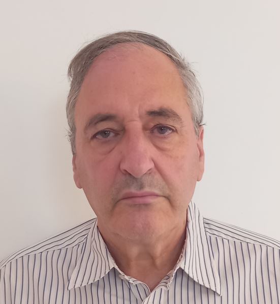
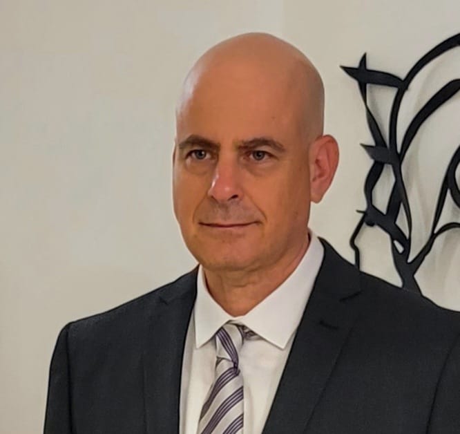
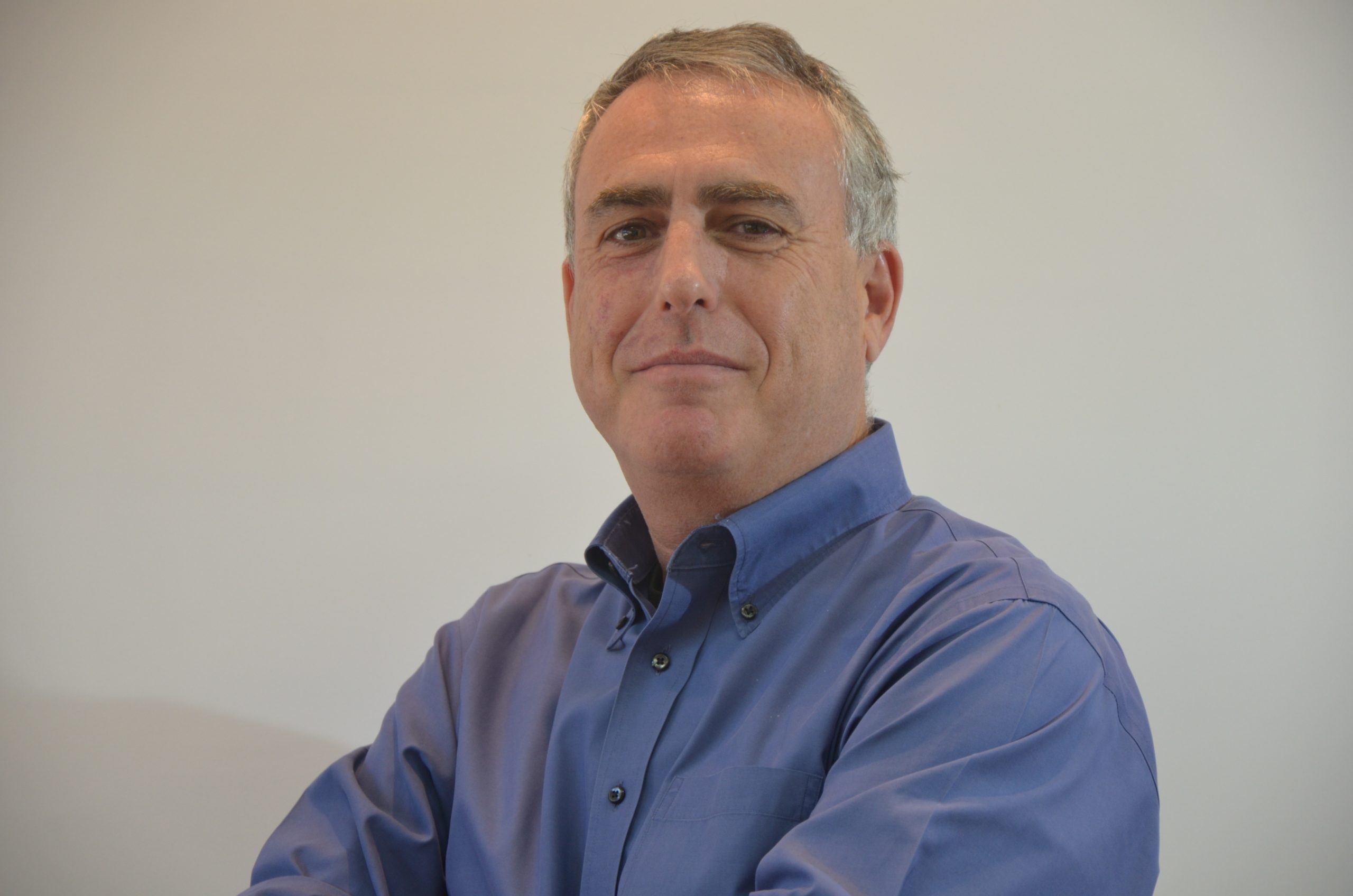
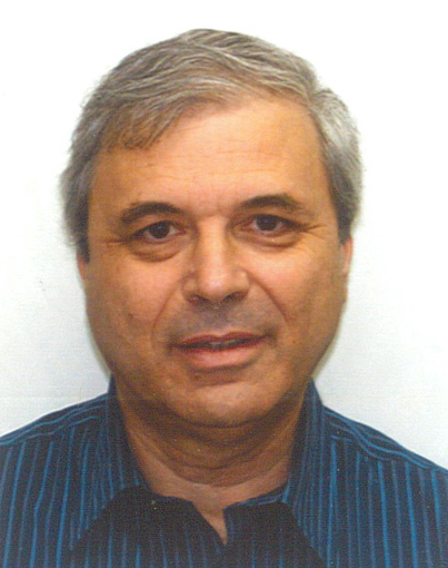
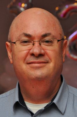
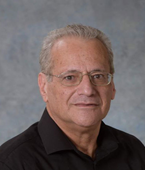
The current research interests of Prof. Ben-Yaakov include power electronics, circuits and systems, electronic instrumentation and engineering education. He published over 300 papers and holds over 30 patents. For over 45 years Professor Ben-Yaakov has been serving as a consultant to commercial companies and governmental agencies in the areas of analog and power electronics and was an entrepreneur and founder of start-up companies. Prof. Sam Ben-Yaakov is a Life Fellow of IEEE


Without proper consideration, EMI can derail projects and create costly delays. With a real-world troubleshooting example, you will learn about basic EMI measurement, common and differential noise sources and identification methods, conducted EMI pre-compliance testing, layout issues, etc.

Design-in of AC-DC front end modules can be complicated. This session will provide a straightforward approach for success, covering such topics as source impedance considerations, inrush current, filter resonance and damping, PFC, faults, fusing, system stability and safety.
Design-in of AC-DC front end modules can be complicated. This session will provide a straightforward approach for success, covering such topics as source impedance considerations, inrush current, filter resonance and damping, PFC, faults, fusing, system stability and safety.
Real-world systems comprise more than just the DC-DC converter itself. Using a case study to examine the requirements of module integration into a DC-DC system, you will learn topics such as input and output filtering, protections, compatibility with the source and load dynamics.
Our experts will share their optimization techniques addressing the following topics: applying thermal models and simulation, PCB layout for effective thermal management, power/signal routing and integrity in high density, high current applications to minimize board losses and maximize performance.
Real-world systems comprise more than just the DC-DC converter itself. Using a case study to examine the requirements of module integration into a DC-DC system, you will learn topics such as input and output filtering, protections, compatibility with the source and load dynamics.


Come and see the OrCAD PCB 3D environment that gives you the ability to see a realistic 3D representation of your design including complex via structures, stackups and isolated sections of the board, mechanical elements and enclosures for true visualization. The environment support 3D placements, 3D checking to detect clashes , 3D flex folding, 3D printing and a lots more. In addition this session will present a seamless co-design integration to ECAD-MCAD mechanical systems supporting IPC-2581/STEP/IDF/IDX implementing an advance push-pull model to eliminate file handling.
Flex and Rigid-Flex substrate are becoming common in areas like IoT, wearables, mobile smart devices, medical devices, automotive and consumers. Come and see how OrCAD PCB handle multiple cross-section materials within different stackups in one design, an area-dependent rules with real-time inter-layer checks to meet rigid-flex manufacturing guidelines that help you to avoid costly fabrication errors, a new flex focus automatic arc routing and a 3D flex bend editor that gives the designer the necessary tools to manage and visualize these complex designs.
PCB designers face significant challenges in integrating RF circuits on a mixed-signal design. Today’s advanced designs are more complex and need to incorporate all design portions such as digital, RF/microwave, and analog circuits on the same board. This session will present an RF design productivity of up to %50 and more using a robust set of layout functionalities to handle complex RF designs like the creation and editing of via arrays and RF etch elements that are parameterized to enable their use in RF circuit design creation including an existing library of more than 600 such parameterized elements from microstrip to stripline to lumped components. And the Flexible Shape Editor (FSE) module that includes a robust set of editing functionality to provides a powerful and flexible adjustment/resizing functions for copper editing to modify RF irregular shapes that used heavily in power amplifier and filter circuits. Also will discuss the interfaces with RF simulation tools like ADS
Post-design DFM checks are too late. Even if you’re able to find a mistake, you’re going to lose hours, days, even weeks adjusting your design. Explore with us OrCAD full DFM, Design for Fabrication (DFF), Design for Assembly (DFA), and Design for Test (DFT) checks that you need in real-time while you design, so you can complete your design fast and signoff with confidence.
The PSpice® Systems Option provides designers with a system-level simulation solution for their designs supporting C/C++/SystemC, and Verilog A-ADM. Designers utilize PSpice simulation programs for accurate analog and mixed-signal simulations supported by a wide range of board-level models. MATLAB Simulink is a platform for multi-domain simulation and model-based design of dynamic systems. PSpice® Systems Option combines industry-leading simulation tools to provide co-simulations, simulation optimizations, parasitic extraction and re-simulation techniques
We will explore the use of Compliance Kit for PCIe 4, USB3, SFP+, MIPI, HDMI and more.These kits come preloaded with various compliance test bench templates to help sign-off analysis get started very quickly. The major compliance checks are built in the compliance kit, eliminating all the work setting up the simulation test criteria.
DDR4 is common high-speed source-synchronous interface. Explore with us DDR4 post-layout simulations with non-ideal power conditions. Synchronous design performance metrics including eye diagrams with detailed timing measurements and compliance kits vs JEDEC standard are available as outputs.
Ensure you get high performance at a system and component level and at the same time save between 15% and 50% in decoupling capacitor (decap) costs. Cadence Sigrity OptimizePI technology does a complete AC frequency analysis of boards and IC packages. Supporting both pre- and post-layout studies, it quickly pinpoints the best decap selections and placement locations to meet your power-delivery network (PDN) needs at the lowest possible cost.
Ensure reliable power delivery within electrical/thermal co-simulation to maximize accuracy. Cadence Sigrity PowerDC technology provides efficient DC analysis for signoff of IC package and PCB designs. PowerDC technology quickly pinpoints excessive IR drop, along with areas of excess current density and thermal hotspots to minimize your design’s risk of field failure.


Euismod, quis laoreet neque imperdiet. Proin ornare, orci eu mattis dignissim, mi mauris consectetur dui, at faucibus libero justo a dui. Sed facilisis pellentesque quam et blandit.
Euismod, quis laoreet neque imperdiet. Proin ornare, orci eu mattis dignissim, mi mauris consectetur dui, at faucibus libero justo a dui. Sed facilisis pellentesque quam et blandit.
Viverra dignissim elit. Maecenas in orci nisl. Cras et nisl aliquet, mollis purus ac, vestibulum metus.

Donec quam felis, ultricies nec, pellentesque eu, pretium quis, sem. Nulla consequat massa qui. Aenean massa. Cum sociis natoque penatibus et magnis dis parturient montes, nascetur ridiculus mus.
Lorem ipsum dolor sit amet, consectetuer adipiscing elit. Aenean commodo ligula eget dolor. Aenean massa. Cum sociis natoque penatibus et magnis dis parturient montes, nascetur ridiculus mus.
Euismod, quis laoreet neque imperdiet. Proin ornare, orci eu mattis dignissim, mi mauris consectetur dui, at faucibus libero justo a dui. Sed facilisis pellentesque quam et blandit.


